
Got news to share with the events industry?
Submit a press release or story tip and reach thousands of event professionals.
Get in touch→More in Semiconductors & Microelectronics
IEEE Spectrum
IEEE Computer Society Chapter Offers Webinars With Industry Experts
Semiconductor Digest
Bosch Establishes Dedicated Semiconductor Division to Strengthen Chip Business
DIGITIMES
SpaceX is reportedly building AI data centers faster than anyone
DIGITIMES
Acer Intelligence Space eyes India growth after strong appliance sales
DIGITIMES
UTI begins iPhone Duo UTG shipments to Samsung Display
Semiconductor Engineering
Fast, Sub-Volt HZO Ferroelectric Capacitors For DRAM-Like Memory (SNU)
Related Insights
 AI infrastructure
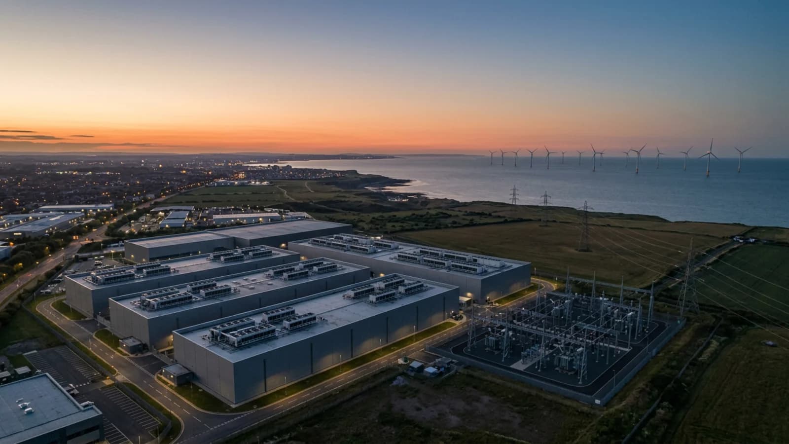
Inside the Cloud, Part 2: The AI Gold Rush Has a Plumbing Problem — and That's Just the Beginning
The expansion of artificial intelligence is creating a much larger industrial economy than most people realize. Behind the computers are energy producers, mining companies, engineers, skilled tradespeople, security specialists, and investors.
20 min read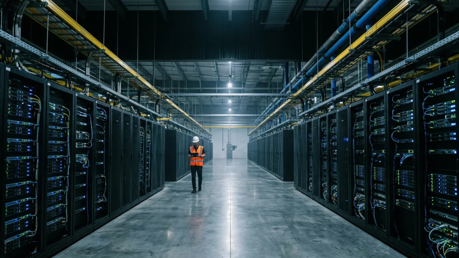 AI infrastructure
Inside the Cloud, Part 1: How Data Centres Are Built, Powered, Cooled and Run
Power, Cooling and 3,000 Workers: How a Data Centre Really Gets Built
20 min read Supply chain intelligence
The Floating Economy: How Tankers and Cargo Ships Quietly Run the World
12.7 billion tonnes of goods cross the oceans a year, yet most people never see the ships. Discover how the tanker and cargo shipping business really works, who owns, builds and crews the fleet, why one strait can shake oil prices, and where the next careers and opportunities are.
24 min read