
Got news to share with the events industry?
Submit a press release or story tip and reach thousands of event professionals.
Get in touch→More in Semiconductors & Microelectronics

Semiconductor Digest
ChipAgents Expands Full-Stack Agentic AI Across Digital and Analog Chip Design
DIGITIMES
China's auto supply chain shifts from price wars to value competition
Semiconductor Digest
Lam and imec Expand Collaboration to Advance Manufacturability of Next-Gen 3D Integration Technologies
Semiconductor Digest
From Lab to Fab: The Rise of HiPIMS in Semiconductor Manufacturing
IEEE Spectrum
How Beta Technologies Is Clearing the Runway for Electric Flight
DIGITIMES
Starlink V3 rollout lifts Win Semiconductors' 2027 satellite outlook as optical communications ramp up
Related Insights
 AI infrastructure
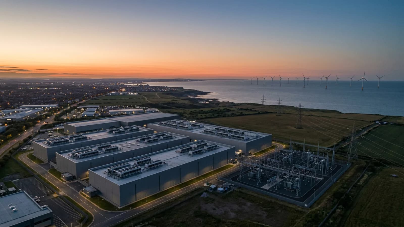
Inside the Cloud, Part 2: The Data Center Economy: The Industrial World Behind Artificial Intelligence
Data centres are now a power, mining and finance story as much as a tech one. See which industries supply them, which depend on them, why China already runs one under the sea, why space is still a long shot, and the five questions investors should ask before backing the boom.
36 min read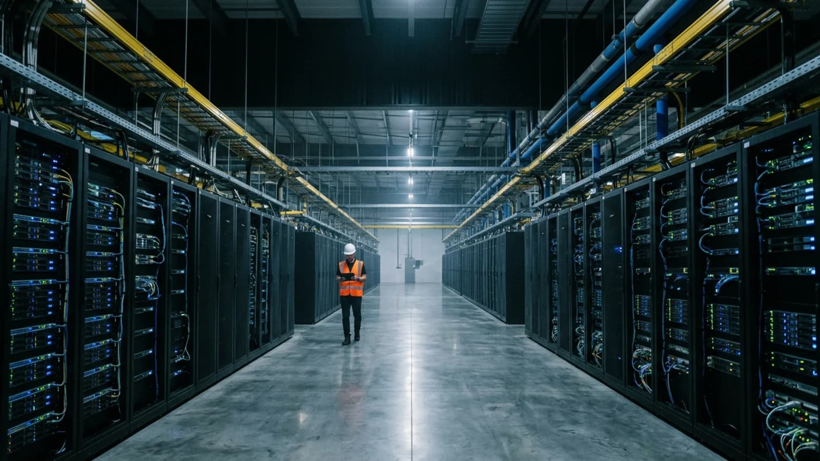 AI infrastructure
Inside the Cloud, Part 1: How Data Centres Are Built, Powered, Cooled and Run
Power, Cooling and 3,000 Workers: How a Data Centre Really Gets Built
20 min read Supply chain intelligence
The Floating Economy: How Tankers and Cargo Ships Quietly Run the World
12.7 billion tonnes of goods cross the oceans a year, yet most people never see the ships. Discover how the tanker and cargo shipping business really works, who owns, builds and crews the fleet, why one strait can shake oil prices, and where the next careers and opportunities are.
24 min read