
Got news to share with the events industry?
Submit a press release or story tip and reach thousands of event professionals.
Get in touch→More in Semiconductors & Microelectronics
EE Times
How Goodram Validates DRAM and SSD Reliability in Europe

Semiconductor Digest
Stacking Up: Inside the Industry’s Race to Build CFET Transistors

IEEE Spectrum
Why AI Can’t Replace Engineering Teams

DIGITIMES
DIGITIMES Insight: BCI grasping reaches market; implant stability and chip heat keep advanced uses beyond 2030

Semiconductor Digest
The Five Factors Defining the Next Generation of AI Inference Chips

DIGITIMES
US signs up to US$389 million in CHIPS R&D deals for power chips and fusion
Related Insights
 Supply chain intelligence
The Floating Economy: How Tankers and Cargo Ships Quietly Run the World
12.7 billion tonnes of goods cross the oceans a year, yet most people never see the ships. Discover how the tanker and cargo shipping business really works, who owns, builds and crews the fleet, why one strait can shake oil prices, and where the next careers and opportunities are.
24 min read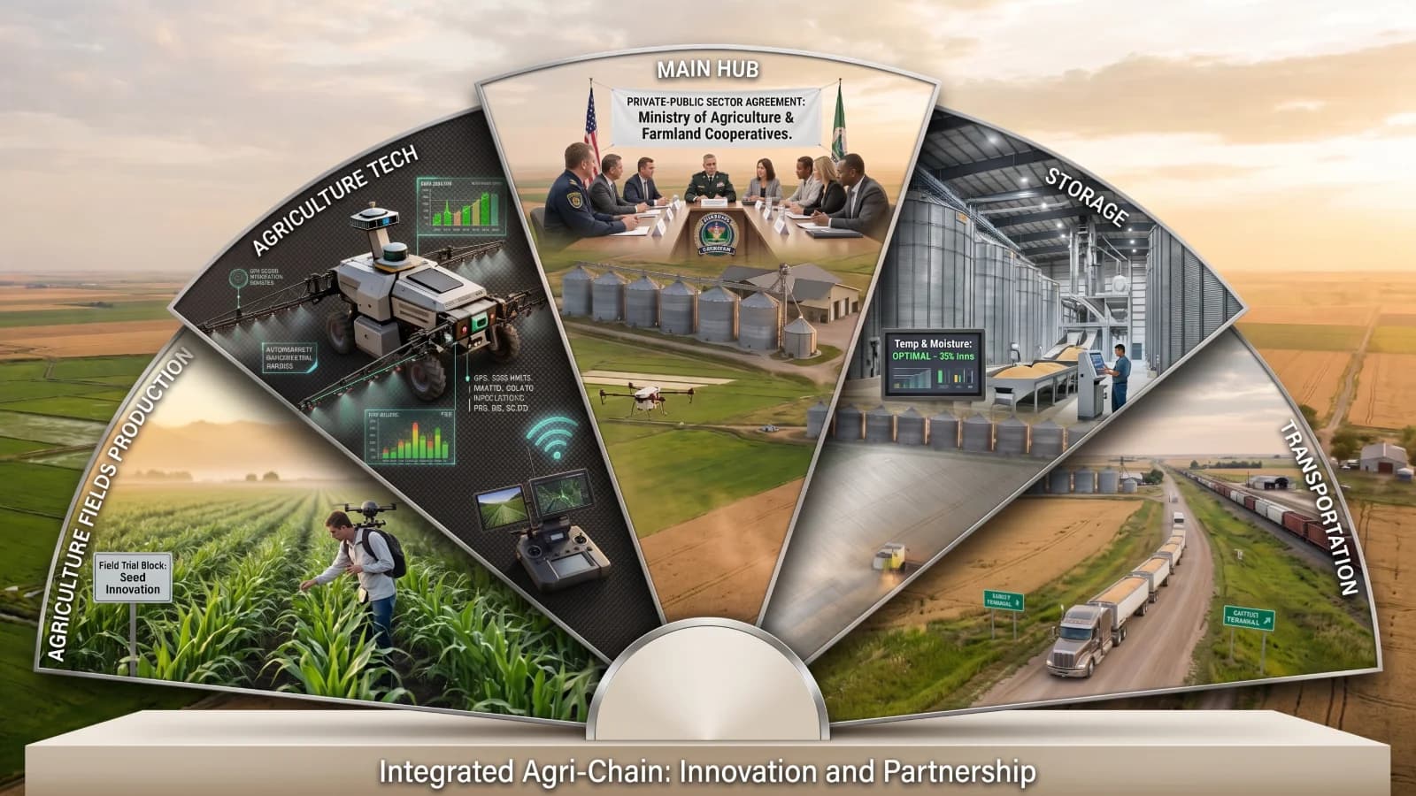 Smart agriculture and food technology
Food = Power
How China Plans to Never Run Out of Food and What the Rest of the World Can Learn
21 min read Clean energy and grid modernization
The Hidden Global Highways of Energy
How Oil, Gas and Power Move Around the World, and Who Keeps Them Flowing
23 min read